Home
Bernard Nysten
Full Professor @ UCLouvain

Main navigation

  • Home
    • About
  • Research
    • Nanomechanics
    • Nanophysics
    • Nanochemistry
    • Team
    • SPM equipements
  • Teaching
    • PhD theses
    • Master theses
    • Courses
  • Publications
    • Theses
    • Book chapters
    • Articles
    • Patents
  • Contact
User account menu
  • Log in

Nanophysics

Profile picture for user Admin_bnysten
By Admin_bnysten, 19 December, 2022

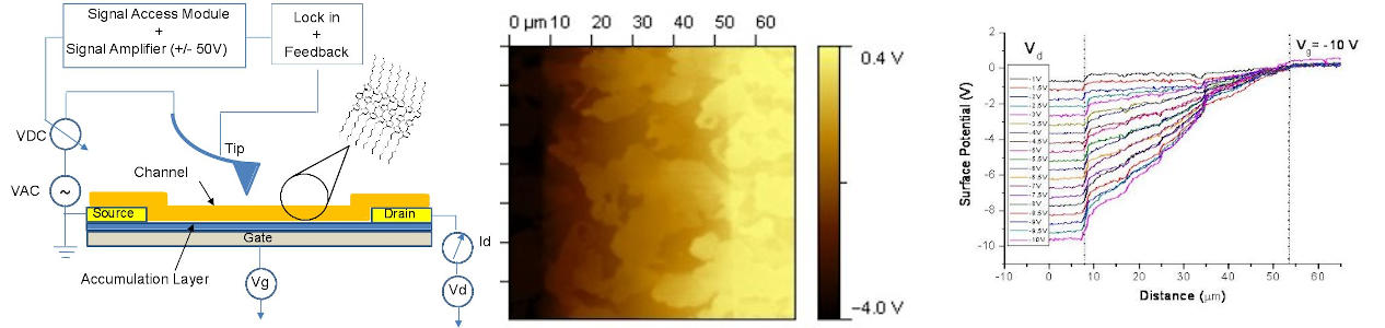
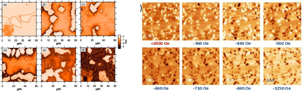
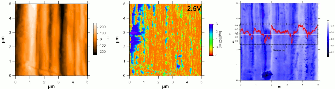
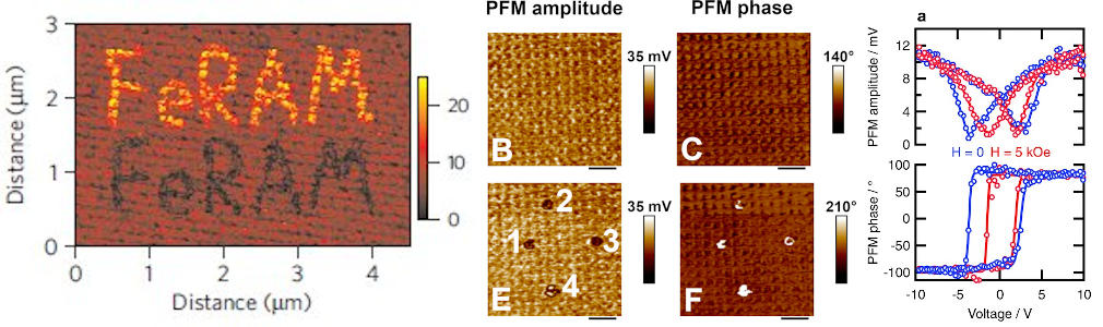
Scanning tunnelling microscopy (STM) and various modes of AFM such as magnetic force microscopy (MFM), electrostatic and Kelvin probe force microscopies (EFM & KPFM), current-sensing atomic force microscopy (CS-AFM) and piezoresponse force microscopy (PFM) were and are used to characterise the physical properties of surfaces and nanomaterials. The topics of these research deal with applications such as organic thin film transistors, charge dissipation in antistatic felts, magnetic structures in high performance steels, magnetic reversal process in arrays of magnetic nanowires, development of plastic ferroelectrics and of magneto-electric hybrid nanostructured layers, ...

STM on terthiophene monolayer
Dioctylterthiophene self-assembled monolayer on MoS2 imaged by STM at the liquid/solid interface (see J. Phys. Chem. C 2013, 117, 21743).
KPFM on OTFT
Kelvin probe force microscopy study of organic thin film transistors: scheme of the experimental setup, KPFM potential image and potential profiles across the channel (see Thin Solid Films 2013, 256, 295).
MFM on steel and Co NWs
Magnetic force microscopy. Left: effect of carburization on the magnetic properties of HP steel (see Scripta Mater. 2008, 59, 1010 & J. Magn. Magn. Mater. 2019, 491, 165578). Right: in-situ study of the magnetic reversal in an array of CoFe nanowires (see J. Superconduct. Novel Magnet. 2013, 26, 1375 & Nanotechnol. 2014, 25, 245707).
CS-AFM and KPFM on steel fibre
Topographic, surface resistance and potential images obtained by CS-AFM and KPFM on a Bekinox fibre used for charge dispersion in antistatic felts (see Appl. Surf. Sci. 2015, 330, 65).
PFM on nanopatterned PVDF-TrFE
Piezoresponse force microscopy. Left: nanoimprinted PVDF-TrFE (see Nature Mater. 2009, 8, 62, Macromol. 2013, 46, 8569). Centre & right: hybrid (Ni nanopillars in imprinted PVDF-TrFE) multiferroic layer with room temperature magnetic switching of the electrical polarization (see Adv. Mater. 2017, 29, 1604604, ACS Nano 2018, 12, 576)

Book traversal links for Nanophysics

  • Nanomechanics
  • Up
  • Nanochemistry

Book navigation

  • Nanomechanics
  • Nanophysics
  • Nanochemistry
  • Team
  • SPM equipements

Research

Researcher on AFM tip
RSS feed

Copyright © 2010, 2025 Bernard Nysten - All rights reserved

Powered by Drupal