Ultra-low-power sensor SoCs for a sustainable IoT
For
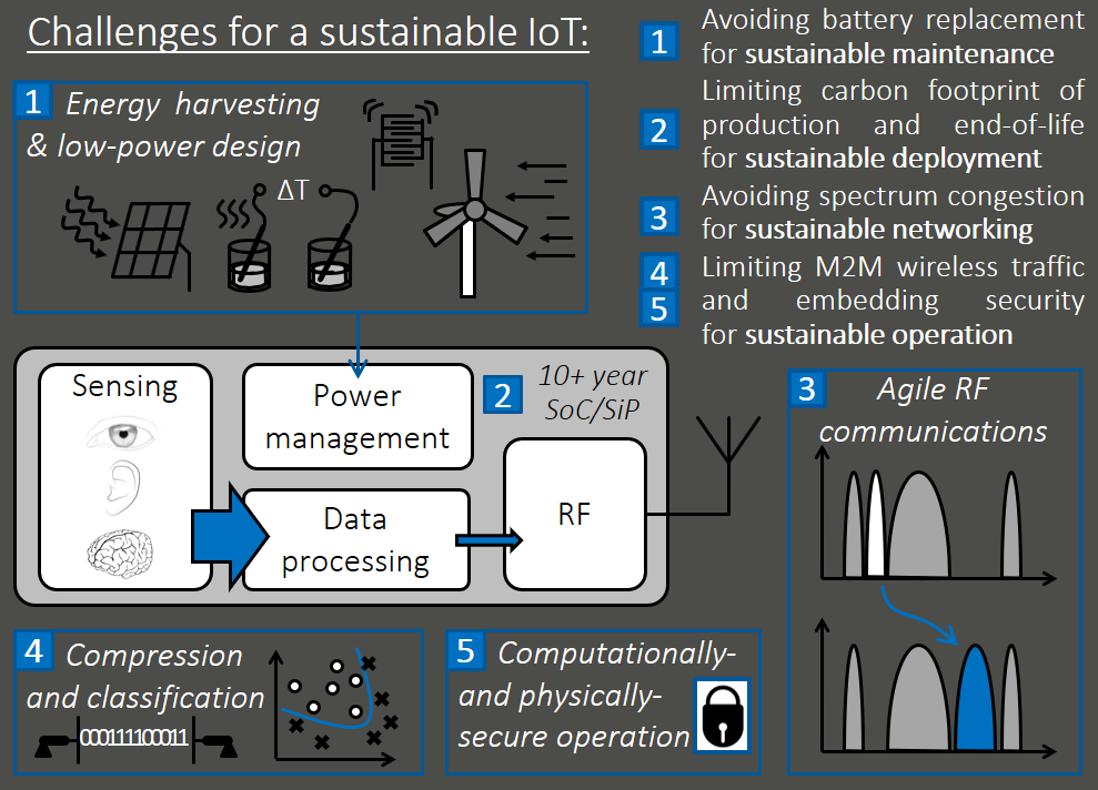
a massive yet sustainable Internet-of-Things, next-generation smart
sensor systems are required to address the five key challenges
represented above [D. Bol, "Can We
Connect Trillions of IoT Sensors in a Sustainable Way ? A
Technology/Circuit Perspective", IEEE S3S Conf., 2015].
Therefore, in the ECS group of UCL, we design ultra-low-power
mixed-signal SoCs featuring the four necessary functions: sensing, data
processing, RF wireless communications and power management. In
order to reach record energy efficiency while preserving
performance, we leverage ultra-low-voltage digital design (ULV
< 0.5V) with all-digital time-based implementation of the analog
functions. A recent overview of latest results can be found here:
[pdf]. |
|
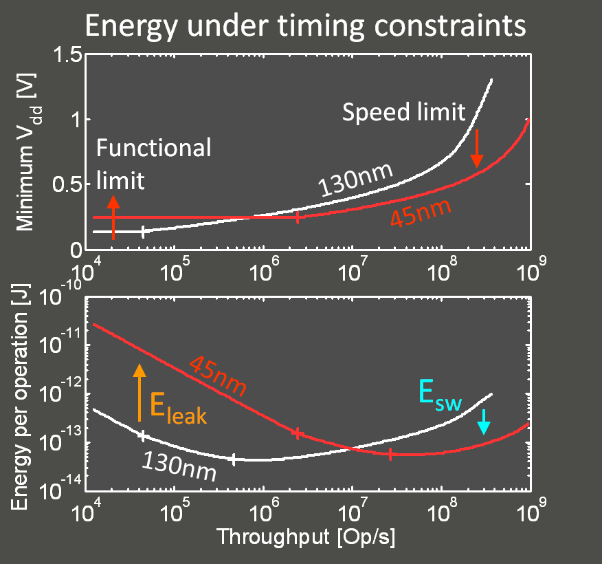
Ultra-low-voltage logic design in nanometer CMOS technologies
Sub/near-threshold
logic is an efficient technique to reduce energy per operation
for
ultra-low-power applications with low-to-medium requirements in speed
performances. Indeed, the operation at ultra-low voltage (Vdd <
Vt)
significantly reduces switching energy. Nanometer CMOS technologies
offer important interests in
terms of reduced swicthed capacitances and supply voltage Vdd to meet a
given
speed contraint. However, implementing subthreshold logic in such
technologies raises important challenges as their typical pitfalls
(leakage current and variability) are magnified by subthreshold
operation. In this context, we target robust and efficient subthreshold
design of logic and memory circuits at full SoC level in nanometer CMOS technologies by
considering :
- technology selection and optimization
(bulk/SOI, MOSFET scaling and tuning, post-CMOS technologies
...),
- standard-cell library design and
characterization,
- timing closure,
- low-power techniques (DFVS, body biaising,
power gating),
- design automation and PVT variations,
- power-management analog blocks,
- circuit/architecture co-design,
- adaptive techniques.
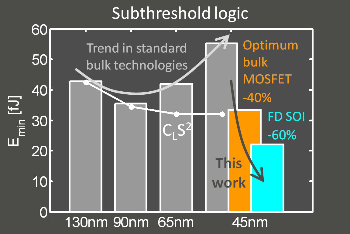
The first full SoC demonstrator of these techniques in Silicon was the SleepWalker SoC (see the chip gallery). Pre-Silicon compact models for simulation of subthreshold logic in 45nm and in 22/20nm
bulk and SOI technologies are available here.
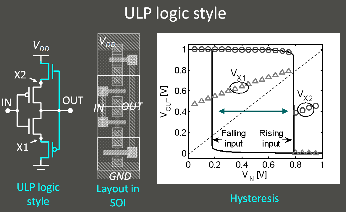
Ultra-low-power
(ULP) logic, memories and sensors
A
disruptive logic style called ULP was proposed based on the ULP
transistor concept (patented) to achieve ultra-low leakage and
high noise margins (above Vdd/2) for logic and SRAM at the expense of
speed performances. Ring oscillator have been demonstrated through
measurements in both bulk and PD SOI 0.13µm technology as well as in
0.15µm FD SOI technology with undoped devices. ULP logic achieves
outstanding leakage current as low as 0.1pA per gate at room
temperature and 30pA per gate at 200°C. Additionally, other circuits
based on the ULP inverter have been, demonstrated in simulation such as
:
- a 1-V 12-T SRAM cell with read noise
noise margin around 700mV,
- an 8-bit 7-kS/s 1-µW interface for
capacitive sensors.
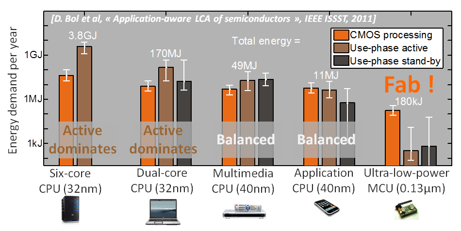
Life-cycle assesment of semiconductors
The
semiconductor industry and the whole ICT market have a high impact on our
environment. We study this impact through life-cycle assesment of
various applications from high-performance (servers and laptops) to
low-power (set-top boxes and smart phones) to ultra-low-power (wireless
sensor nodes, biomedical, RFIDs). We showed that the life-cycle phase
with the highest impact strongly depends on the applications.
|